Before designing multi-layer PCB circuit boards, designers need to confirm the circuit boards structure primarily based on the scale of circuit, the size of circuit boards, and the requirements of electromagnetic compatibility (EMC). It means that designers have to decide to use 2, 4, 6, or more layers of circuit boards. If the design requires the use of high density ball grid array (BGA) devices, the minimal number of wiring layers required for these devices must be considered. For years, people always believe that the less PCB layers, the lower the cost, however, there are many other factors affecting PCB manufacturing costs. In recent years, the differences between costs of multi-layer boards have been reduced significantly. As soon as the number of layers been determined, the placement of the inner layer and how to distribute different signals in these layers can then be decided --- this is the stack-up design of multi-layer PCB. Careful planning and choosing rational stack-up designs beforehand will save a lot of efforts in the following wiring and future production.
1.1 Layer Selection Principle
There are many factors to consider when determining the number of layers of multi-layer PCB board. For experienced designers, they will
emphasize on the analysis of the bottlenecks of PCB wiring after the pre-placement of devices. In combination with other EDA tools to analyze wiring density of circuit board; and combined with the quantities and kinds of signal lines with specific wiring demands, such as differential lines, sensitive signal lines, to determine the number of signal layers; and then to determine the number of internal power layer according to the type of power supply, isolation and immunity requirements. Therefore, the layer number of the whole circuit board plates is basically determined.
The following table is the empirical data to determine number of signal layers based on the PIN density, for reference.
Ps: Definition of PIN density: Area of board (square inch)/ (Total number of pins on the Board/14)
1.2 PCB Stack-Up Principle
After the number of circuit board layers determined, the following job is to reasonably arrange the placement order of the circuit of each layer. In this part, there are two main factors to be considered:
(1) The distribution of special signal layers
(2) The distribution of power layer and ground layer
The more layers of circuit boards, the more varieties of arrangement of special signal layers, ground layers and power layers, thus it is more difficult to choose the best combination method, but the general principles are as follows.
(1) The signal layer should be next to an internal power layer (internal power/ground layer), shielded by the copper film of internal power layer.
(2) The internal power layer should be integrated with ground layer tightly, which means the thickness of medium between internal power layer and ground layer should take the smaller value, in order to improve the power supply capacitor between the internal power layer and ground layer, and increase the resonant frequency. If the electric potential difference between internal power layer and ground layer is not significant, a smaller insulation thickness can be used, like 5mil (0.127mm).
(3) To avoid the two signal layers directly adjacent. It is easy to introduce crosstalk between adjacent signal layers, leading to the fail of the circuit. To place a ground layer between two signal layers can avoid cross talk efficiently.
(4) Multiple grounded internal power layers can reduce the ground impedance effectively. For example, A signal layer and B signal layer use ground plane respectively can reduce common-mode interference effectively.
(5) The symmetry of layer structure.
1.3 Demonstration
For your reference, a stack-up design for the four, six, and eight layered high speed digital signal PCB is demonstrated in below:
1.3.1 Four Layer Stack–Up

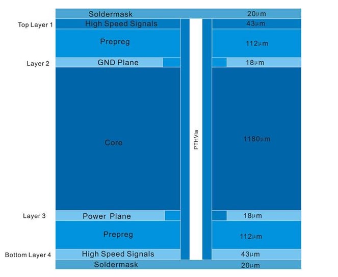
Figure 1.3.1 Four Layer PCB Stack-Up Example
The high speed signals on the top layer are referenced to the ground plane on layer 2. Since the references for the high speed signals on the bottom layer are the power planes on layer 3, it is necessary to place stitching capacitors between the aforementioned power planes and ground. In this stack up, it is preferential to route high speed signals on the top layer as opposed to the bottom layer so that the signals have a direct reference to the ground layer. For some designs it may be desirable to have the bottom layer as primary high speed routing layer. In this case, the power and ground usage on Layer 2 and 3 could be swapped.
1.3.2 Six Layer Stack-Up

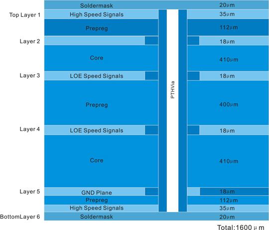
Figure 1.3.2 Six Layer PCB Stack-Up Example
In this example, the reference planes for the high speed signals on the top layer are the power planes on layer 2. Stitching capacitors from
the associated reference power plane to ground are therefore required. The signal reference for the bottom layer is the ground plane on layer 5. In this stack-up, it is preferable to route high speed signals on the bottom layer. As in the previous example, power and ground layers could be swapped if it is desirable to have the primary high speed routing layer on the top layer.
The reference planes for signals on layer 3 are located on layer 2 and 5. The same reference planes are used by signals routed on layer 4. As the reference planes are on layers which have a relatively large distance from signal layers 3 and 4, the traces would need to be very wide in order to achieve a common impedance of 50Ω. Therefore, these layers are not suitable for routing high speed signals. In this stack-up approach, layers 3 and 4 can only be used for routing low speed signals where impedance matching is not required.
1.3.3 Eight Layer Stack-Up

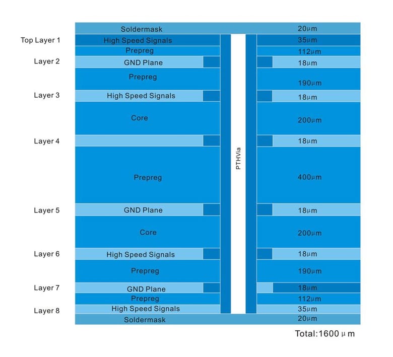
Figure 1.3.3 Eight Layer PCB Stack-Up Example
The signals on the top layer are referenced to the plane in layer 2, while the signals on the bottom layer are referenced to layer 7. The reference planes for signal layer 3 are the ground plane on layer 2 and the power planes on layer 4. When routing high speed signals on layer 3, stitching capacitors need to be placed between the power and the ground planes. The power planes on layer 5 and 7 are used as references for the high speed signals routed on layer 6.
The inner layer 6 with the two adjacent ground planes is the best choice for routing high speed signals which have the most critical impedance control requirements. The inner layers cause less EMC problems as they are capsulated by the adjacent ground planes. As layer 3 is referenced to a power plane, outer layer 1 and 8 are preferable for high speed routing if layer 6 is already occupied.
If you want to learn more about PCB design, we highly recommend you to check the following articles:
- Fundamental Technological Requirements of PCB Design
- Screen Printing Design
- How to create a PCB stencil File
- Panel Design
- Design of Hole
- Bonding Pad
- What is a Gerber file?
Our engineers at NexPCB are professionals in making sure that all of these variables are taken into account for our customers projects. Let our team help you with your next PCB project!
Posted by NexPCB United

Anything that was written as a group effort is added here. One for all, all for one!

